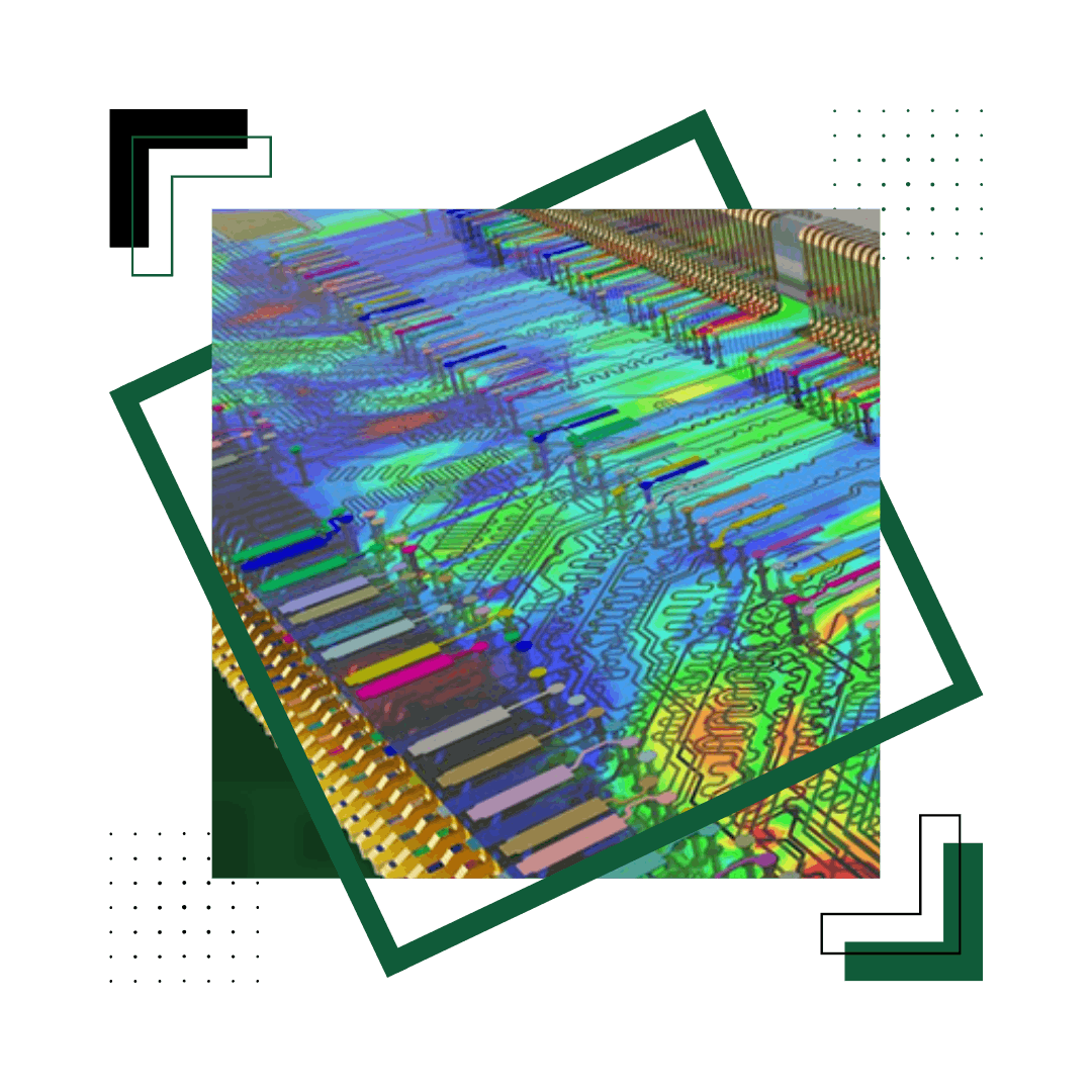
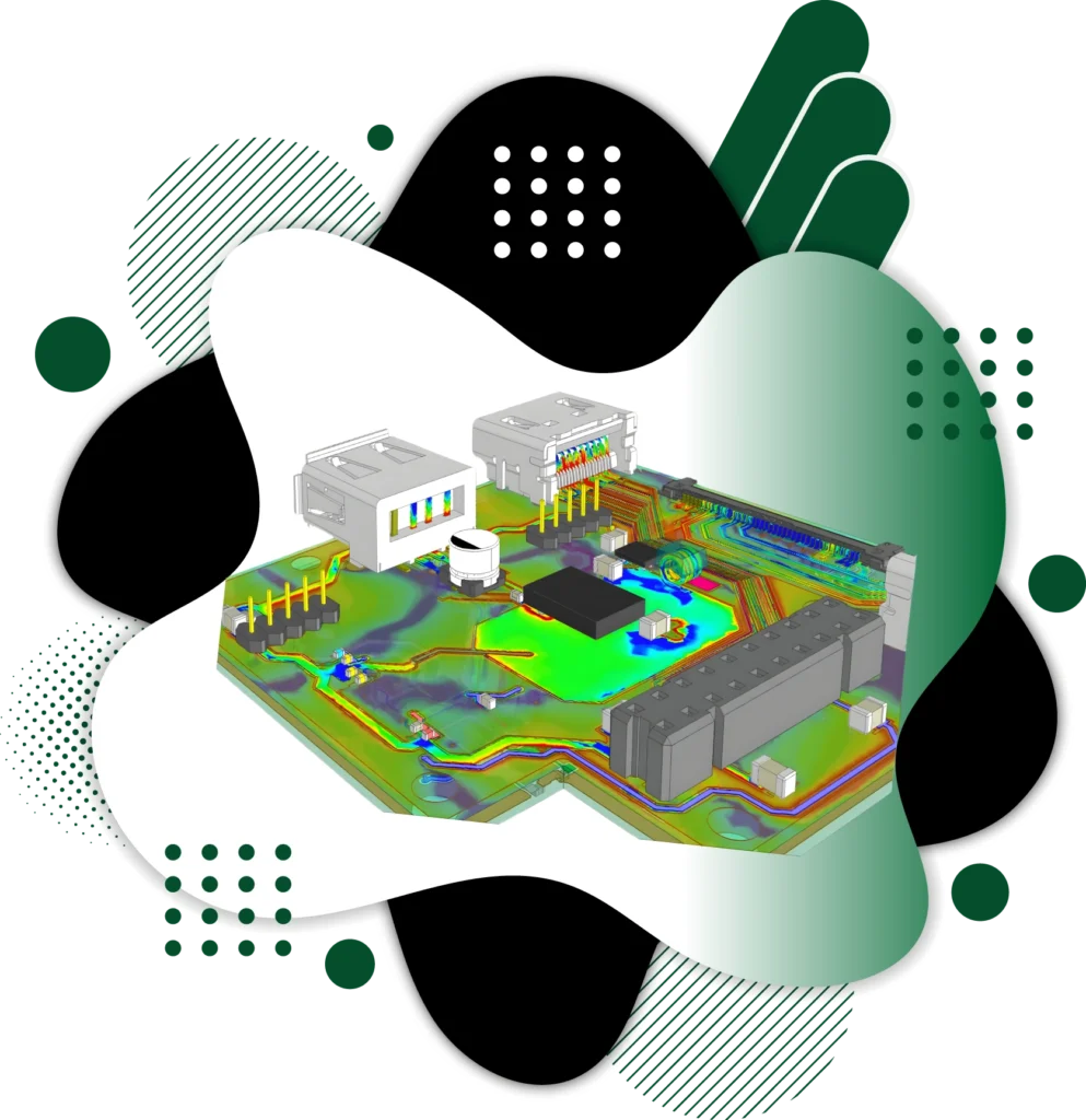
PCB SIMULATION & ANALYSIS
We help you simulate and eliminate the signal, power, thermal, & EMI/EMC risks.
We run signal integrity simulations to spot quality issues and power integrity analysis to ensure stable power delivery.
At TechiesDesigns, we’re obsessed with the details that keep hardware running specifically Signal Integrity, Power Integrity, EMI/EMC ,and Thermal Analysis. We know that behind every great product is a PCB that needs to stay cool, quiet, and reliable.
We don’t just “check” your boards; we dive deep into the simulations to catch signal loss, noise, and overheating before they become expensive physical headaches. Our goal is to give you total confidence in your hardware’s performance, so by the time it hits the enclosure, you know it’s going to work exactly as intended.
Engineering roadmaps are stressful enough without SI or Thermal issues slowing you down. Whether your team is hit with a peak workload or you just need a specialized set of eyes for a tough project, we step in to provide that high-level expertise fast, flexible, and without the overhead of a full-time hire.
Why Choose TechiesDesigns For PCB Simulation & Analysis?
We Offer the Full Spectrum of Advanced PCB Simulation and Analysis.
Signal Integrity
Simulations to identify and address potential signal quality issues.
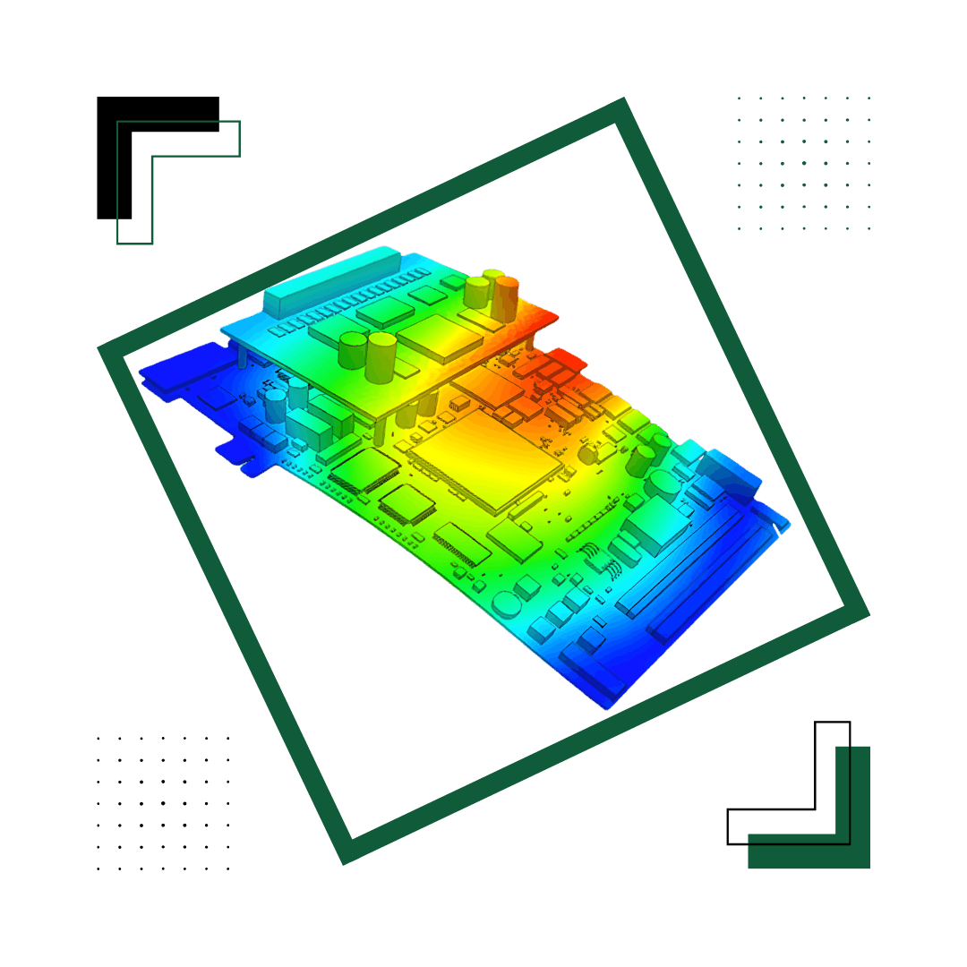
Power Integrity
Analysis to ensure stable power delivery across the board.
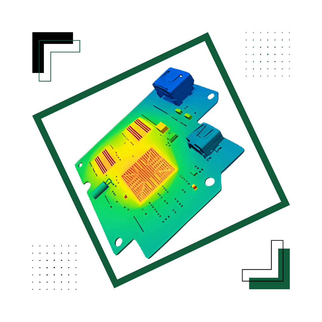
Thermal Analysis
Simulates heat dissipation and temperature management.
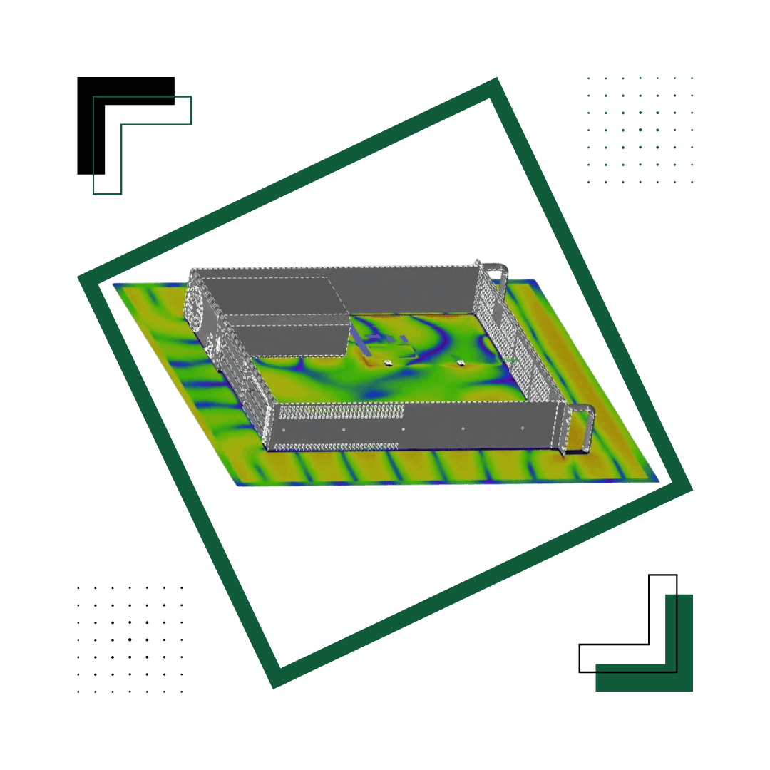
EMI/EMC
Analysis to ensure minimal electromagnetic interference and resilience to external noise.
SIGNAL INTEGRITY ANALYSIS
We evaluate signal behavior and logic rise/fall times to eliminate costly PCB design iterations, safeguard product integrity, and deliver fault-free circuit designs.
In today’s landscape of increasingly compact electronics and higher clock speeds, signal integrity has emerged as a paramount concern for high-speed digital design. Conducting thorough signal integrity analysis is essential for any high-speed project, as it enables detailed verification of high-speed signals on the printed circuit board (PCB) during the design phase. This proactive approach substantially reduces errors in the final product, minimizes time spent on testing and debugging, and brings products to market faster. Critically, signal integrity analysis can be integrated into an organization’s existing design process with minimal disruption, making it a highly practical addition to any development workflow.
PCB Signal Integrity is conducted in two steps
Pre Layout PCB SI Analysis Check
➥ Placement optimization, Trace length constraints.
➥ Impedance requirement.
➥ Topology and termination strategies.
Post Layout PCB SI analysis check
➥ Verification by extraction of the actual PWD parasitic.
➥ Placement optimization based on signal flow & trace length requirement of the specific interface.
➥ Layer stack-up recommendation.
➥ Reflections analysis and determination of termination scheme.
➥ Generation of PCB layout constraints & guidelines.
➥ Delay & Timing determination.
➥ Crosstalk level estimation.
➥ Eye diagram analysis.
Capabilities Of Signal Integrity Analysis
-
Reflection Waveform Analysis
➥ Identifies signal reflections due to impedance mismatches to ensure clean, reliable high-speed signal transmission.
-
Crosstalk Analysis
➥ Evaluates unwanted signal coupling between adjacent traces to minimize noise interference and ensure signal integrity in high-speed PCB designs.
-
Propagation Delay and Timing Analysis
➥ Measures signal travel time and timing relationships to ensure proper synchronization and reliable interface performance.
-
Eye Diagram Analysis
➥ Evaluates signal quality by analyzing eye opening, jitter, and noise to ensure reliable high-speed data transmission.
Power INTEGRITY ANALYSIS
Power Integrity analysis helps you to assess the potential threats to device operability and identify options for resolving bottlenecks. This study allows us to estimate factors such as voltage drop at each point of the network, interconnect temperature rise, plane noise level, and others. This evaluation frequently shows several difficulties that may be prevented and allows for the development of solutions aimed at enhancing design.
TechiesDesigns can do high-quality Power Integrity PCB examination and provide the simplest remedies for potential problems. As a result of our efforts, we deliver a full Power Integrity report outlining the issues and suggestions for improving the design. Certainly, it will help you considerably enhance the quality and lower the cost of your item.
Capabilities Of Power Integrity Analysis
-
Decoupling Analysis
➥ Analyzing the impedance of the power distribution network at multiple board locations and suggesting proper decoupling schemes.
➥ PCB layout Stack up suggestions for proper board decoupling.
➥ Frequency versus Impedance plot. -
DC Noise Analysis
➥ Simulation of plane noise due to improper decoupling schemes.
➥ A 3D plot of plane noise.
-
DC Drop Analysis
➥ Modeling Power Plane structures to validate IR/DC drop in power supply.
Rails due to copper losses.
➥ Output available in the form of a report indicating current flow and voltage at each power pins of circuit devices.
➥ 3D Plots generation representing voltage distribution through the power planes.
➥ Current density 3D plot.
THERMAL ANALYSIS
Thermal management is an important part of printed circuit board (PCB) design. A PCB’s temperature profile is determined by its power dissipation and distribution of heat-generating components, as well as the overall board structure. Overheating can cause performance concerns, reduced dependability, and even full failure.
Thermal modeling enables the prediction of temperature distribution across the PCB as well as the identification of hot spots. This allows the design to be optimized so that components remain within their safe operating temperature range. This article gives a detailed approach on thermal modeling and simulation for printed circuit boards.
Capabilities Of Thermal Analysis
-
Steady-State Thermal Simulation
➥ Steady-state simulation simulates the board in equilibrium, with components dissipating power over time. It depicts the total temperature distribution over the PCB once heat flow has stabilized for a significant amount of time.
➥ Steady-state analysis is rapid and gives a thorough insight of overall thermal performance. It is widely utilized throughout the early design stages.
-
Transient Thermal Simulation
➥ Transient simulation describes the board's dynamic thermal response to power cycling over time. The temperature profile is evaluated since heat varies when devices are turned on and off during normal operation.
Rails due to copper losses.
➥ Transient analysis can detect peak temperatures and time-dependent effects. It provides a deeper insight and is done later in the design process.
Electromagnetic interference & compatibility (EMI/EMC)
Electromagnetic interference (EMI) and electromagnetic compatibility (EMC) are critical considerations in modern PCB design. As high-speed electronics become increasingly complex, ensuring that printed circuit boards operate reliably without disturbing nearby systems or being affected by external electromagnetic noise has become non-negotiable. These challenges demand a deeper understanding of real-world electromagnetic behavior, beyond what traditional design approaches can predict.
EMI/EMC testing forms the foundation for meeting global regulatory requirements such as FCC, CE, and IEC, while also ensuring consistent and dependable performance in practical operating conditions. By identifying potential risks early and validating designs before production, it helps minimize costly redesigns, prevent compliance failures, and deliver products that perform exactly as intended in the environments they are built for.
Capabilities Of EMI/EMC
-
PCB and Enclosure Analysis
An entire circuit board model, including stackup, dielectric characteristics, metallization, vias, and components, is created beginning with layout files. In PCB modeling, a few items of particular significance for EMI analysis are as follows:
➥ Fast signal routing.
➥ Power supplies in switch mode.
➥ Resonances in the ground and power plane cavities.
➥ Decoupling the routing and positioning of capacitors.
➥ Filters and additional circuits.
➥ Board enclosure and return path connection.
Engineering Success Stories: PCB Analysis in Action Case Studies
We provide Detailed Simulation and Verification Report.
