PCB FABRICATION
From Design Files to Physical PCBs.
Delivering High-Quality, Cost-Effective, and Fully Compliant PCBs for Every Application.
Printed Circuit Boards are the backbone of modern electronics. A product’s efficiency and long life are determined by the reliability of its PCB. As a leading PCB manufacturer and supplier, we deliver high- performance circuit boards for diverse electronic industries around the world.
At TechiesDesigns, quality is our priority, ensuring every PCB leaving our facility performs reliably. Every board we fabricate is designed to meet stringent electrical, mechanical, and environmental standards, ensuring your products perform flawlessly.
Our PCB fabrication services cover single-layer to multi-layer boards, utilizing high-quality materials, advanced surface finishes, and industry-standard processes. With end-to-end quality control, including electrical testing, visual inspection, and traceability, we ensure each PCB meets your exact requirements, from rapid prototypes to high-volume production. We deliver consistent, reliable PCB solutions tailored to your application. By combining advanced technology, engineering expertise, and customer-focused processes, we enable seamless electronics production on time.
Why Choose TechiesDesigns For PCB Fabrication Service?
High-Quality PCB Fabrication Solutions with Reliable Lead Times - from Prototype to Mass Production.
-
Precision Engineering
We manufacture PCBs with precise layer registration, controlled impedance, and optimized trace geometries ensuring electrical performance that matches your design intent.
-
Advanced Materials & Manufacturing
From single-layer to complex multi-layer boards, we work with FR-4, aluminum, and high-TG materials, supported by industry-standard surface finishes such as HASL, ENIG, and OSP.
-
Standards-Driven Quality
Every PCB undergoes rigorous quality control, including electrical testing, visual inspection, and complete lot traceability to ensure long-term reliability and consistent performance.
-
Reliable & Flexible Lead Times
Whether you need rapid prototyping or volume production, our optimized workflows ensure on-time delivery without compromising quality or process control.
-
Cost-Optimized Fabrication
Our streamlined manufacturing processes deliver competitive pricing while maintaining precision, yield consistency, and product reliability.
-
End-to-End Project Support
From design review and manufacturability guidance to final production and delivery, we provide clear communication, technical assistance, and a smooth production experience.
-
Customization Backed by Top Experts
We support specialized PCB requirements including HDI, controlled impedance, thermal management, and environment-specific designs guided by experienced engineering support.
-
Sustainability & Regulatory Compliance
We follow environmentally responsible manufacturing practices using lead-free processes, RoHS-compliant materials, and energy-efficient production methods to meet global regulatory standards.
01. Rigid PCB
| SN | DESCRIPTION | TECHNICAL CAPABILITIES |
|---|---|---|
|
01 |
Standard |
IPC-A-600 Class 2
|
|
02 |
Layer Count 1–24 |
IPC-2221 / IPC-2222 |
|
03 |
Maximum Board Size |
480 X 380 mm |
|
04 |
PCB’s thickness |
0.2 mm to 10 mm |
|
05 |
Heavy Copper Thickness
|
140 microns |
|
06 |
Minimum Line Spacing |
4 mils |
|
07 |
Minimum Line width |
4 mils |
|
08 |
Minimum plating thickness in holes |
4 mils |
|
09 |
Impedance Control |
Single and Differential |
|
10 |
Materials |
➥ Nanya plastic (NP140TL,NP155FR, NP175FR,NY1140,FR486- 140Tg,NY2170) ➥ ISOLA (ED130UV-135Tg,FR402-140Tg,IS400-150 Tg,IS410- 180 Tg,185HR-180Tg,370HR-180Tg) ➥Wazam (H1170-170Tg, H140A-130Tg, H150-150Tg) |
|
11 |
Special Material |
Rogers 4000 |
|
12 |
Surface Finishes |
LF-HASL, HASL, ENIG, OSP, Immersion Silver, Immersion Tin, Hard Gold |
|
13 |
Solder Mask Color |
Matte Green, Standard Green, Black, White, Blue, Red, Yellow |
|
14 |
Legend Color |
Black and White |
|
15 |
Panel Cutting Types |
V cut & CNC Routing |
|
16 |
Special PCBs |
Blind and Buried Vias, Half PTH Castellated holes, Edge Plating |
02. Metal Clad PCB
| SN | DESCRIPTION | TECHNICAL CAPABILITIES |
|---|---|---|
|
01 |
Thermal conductivity |
1 W/mK, 2 W/mK, 3 W/mK, 5 W/mK, 10 W/mK, 12 W/mK |
|
02 |
Thermal resistance |
≤ 1.0 °C/W |
|
03 |
Maximum Board Size |
1200 × 350 mm |
|
04 |
PCB’s thickness |
0.2 – 2.0 mm |
|
05 |
Surface finish |
Lead HAL, Lead-Free HAL, OSP, ENIG |
|
06 |
Solder mask color |
White |
|
07 |
Base material |
Aluminum TC1 / TC2 |
|
08 |
Copper thickness |
1 oz / 2 oz / 3 oz |
|
09 |
Thermal dielectric thickness |
75 µm / 100 µm / 150 µm |
|
10 |
Aluminum base thickness |
0.8 mm / 1.0 mm / 1.5 mm / 2.0 mm |
|
11 |
Legend Color |
Black |
03. Flex PCB
| SN | DESCRIPTION | TECHNICAL CAPABILITIES |
|---|---|---|
|
01 |
Standard |
IPC-6013 Class 2 |
|
02 |
Layer Count 1-2 |
IPC-2223 |
|
03 |
PCB’s thickness |
0.06mm/ 0.11mm |
|
04 |
Materials |
Polyimide ( Tg230) |
|
05 |
Solder mask |
Yellow |
|
06 |
Surface finish |
Only Copper, ENIG, Immersion Tin |
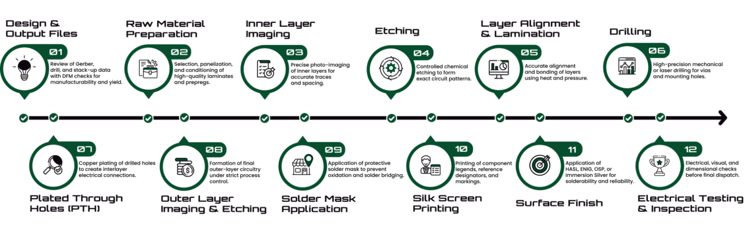
Our PCB Fabrication Workflow
Get Your PCB Fabrication Quote Now
Our PCB Inspection Methods
➥ Visual Inspection
Manual or automated surface inspection to detect visible defects such as scratches, misalignment, or solder mask issues.
➥ Sample Lot Inspection
Random sampling of production batches to validate process consistency and quality.
➥ Tin Sample Inspection
Examination of solder pads to verify tin thickness, adhesion, and solderability.
➥ E-Test (Electrical Test)
Flying Probe for low–medium volumes and Bed-of-Nails for high volumes to verify continuity, shorts, and opens.
➥ Cross-Section Analysis
Sectioning and microscopic analysis to check layer alignment, via plating, and lamination integrity.
➥ Impedance Coupon Test
Measurement of dedicated test coupons to confirm controlled impedance for high-speed designs.
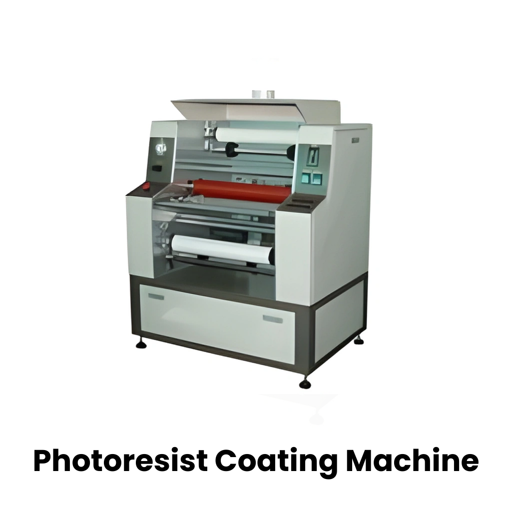
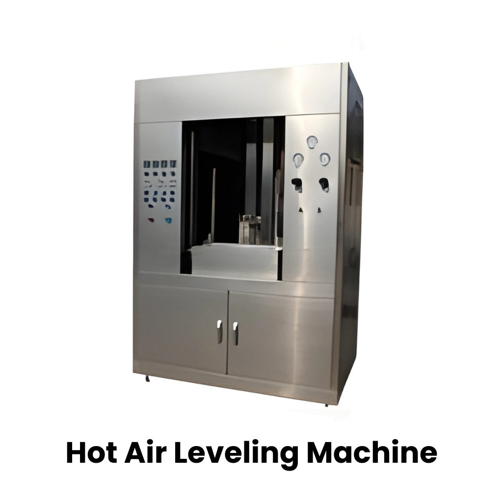
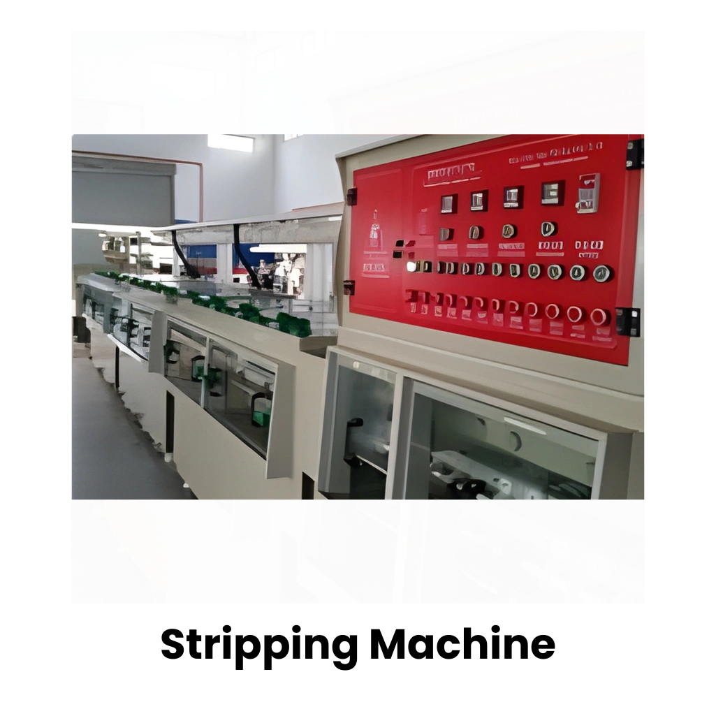
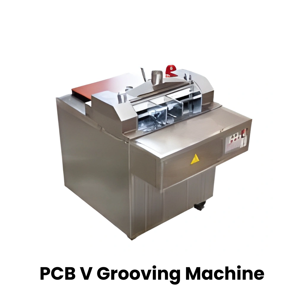
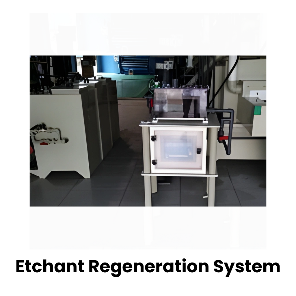
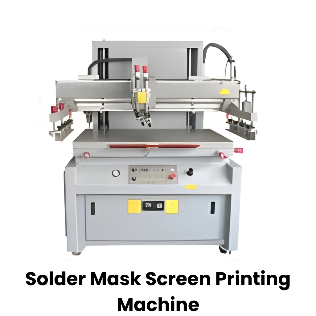
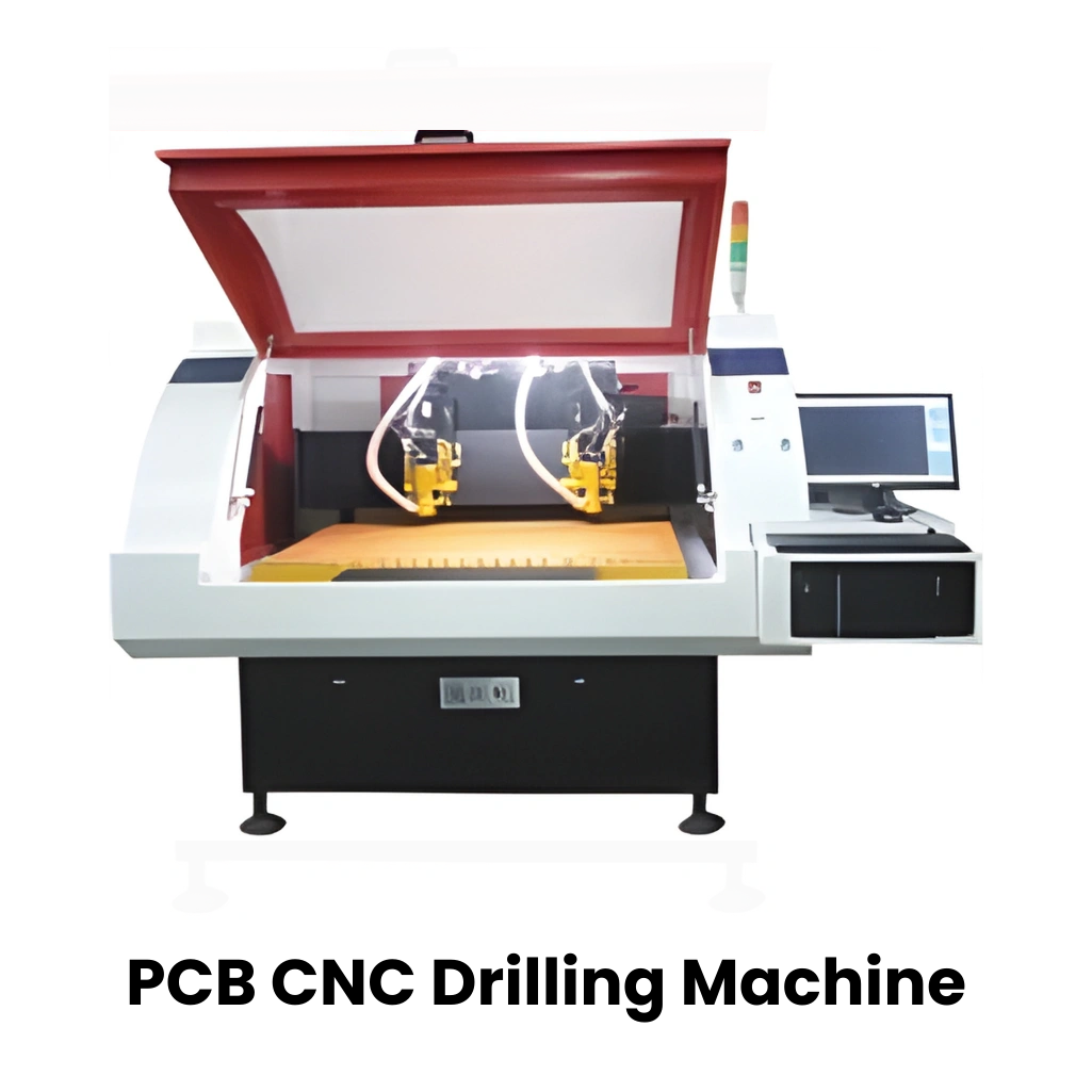
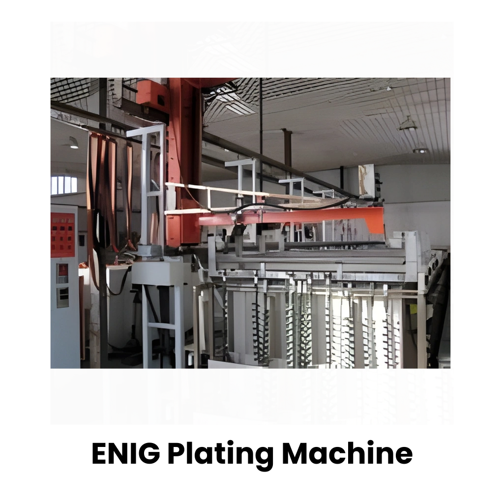
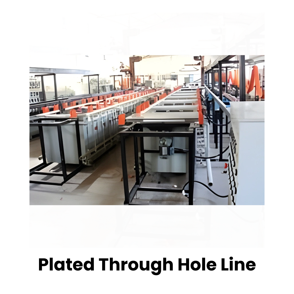
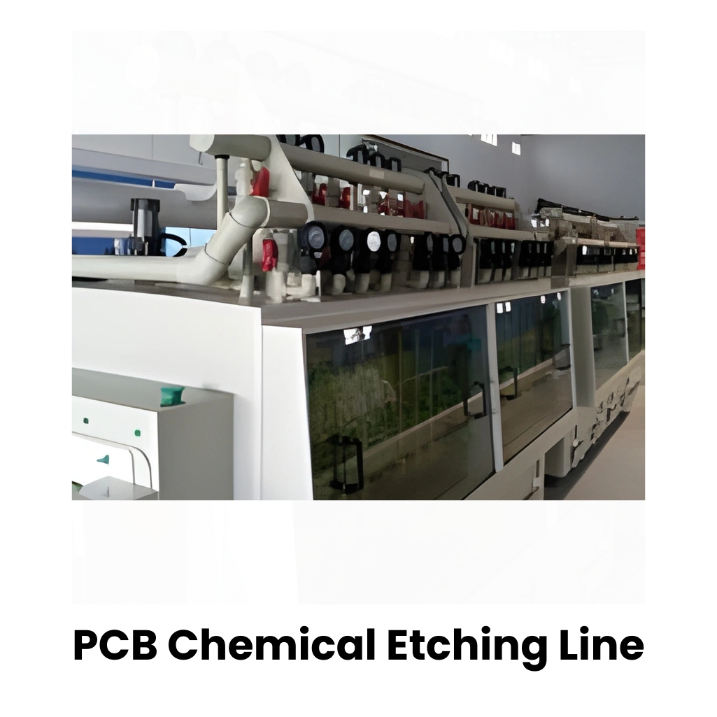
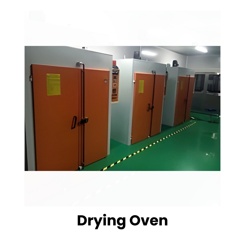
Our PCB fabrication infrastructure
Printed Circuit Board Manufacturing Process & Equipment
- Automated Optical Inspection [AOI]
- Pre-production Engineering Team
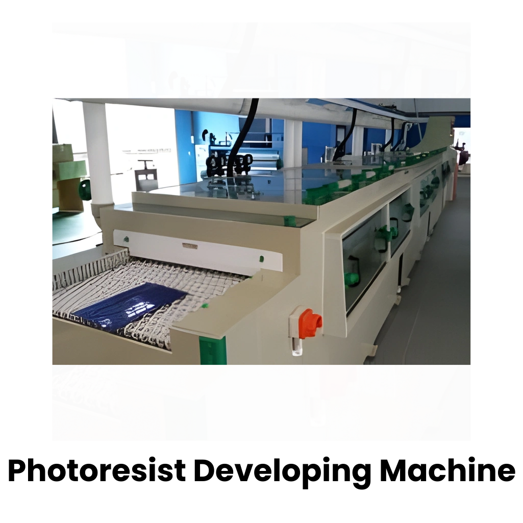
- Photo plotter - Photographic film processor
- Impedance Control Testing Machine
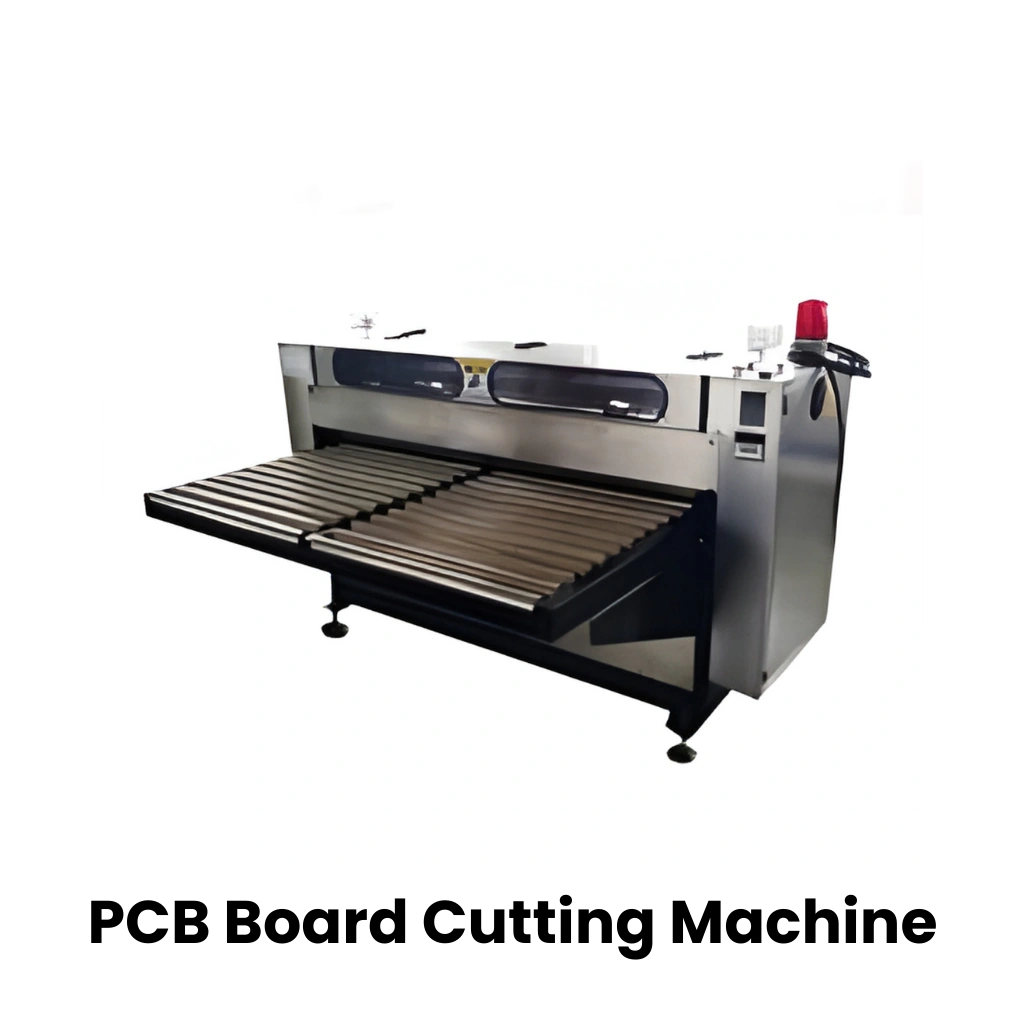
- PCB Board Cutting Machine
- Inner layer registration welding machine
- Multi-layer vacuum lamination (pressing)
- CNC drilling machines - 7 spindles
- CNC routing machines - 4 spindles
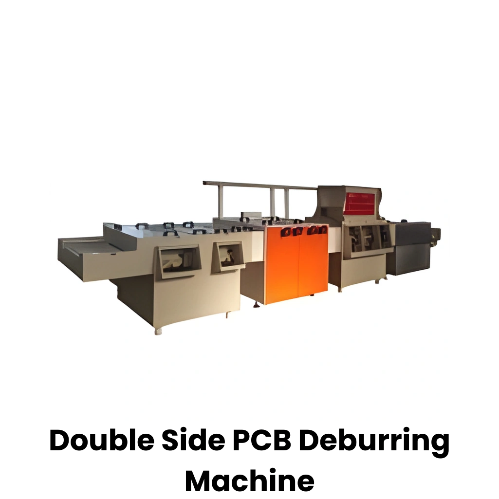
- Automatic PCB Grinding Brushing Machine
- Desmear Electroless Automated Line
- Dryfilm photo resist laminator
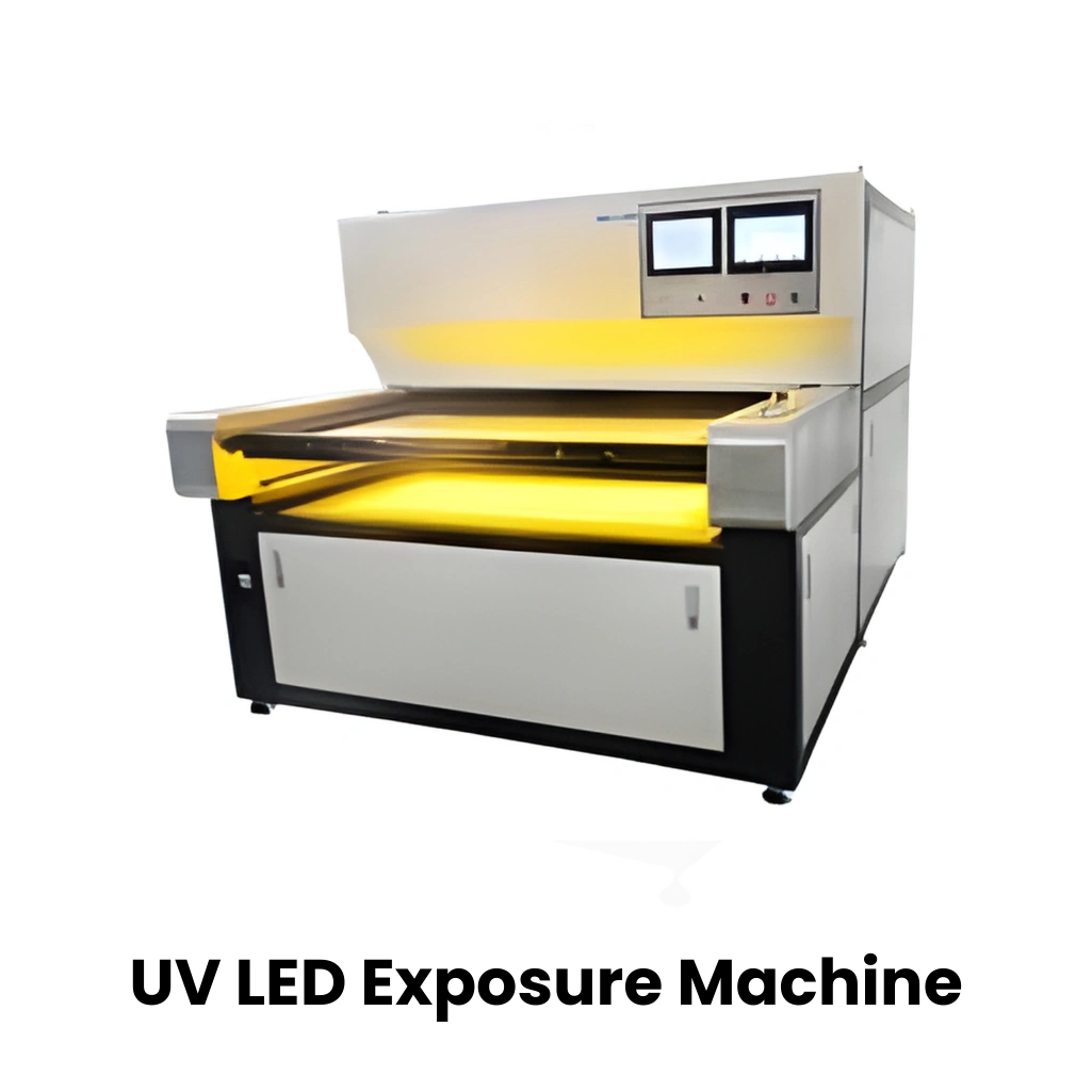
- Imaging- Laser Direct Image
- Electroplating copper and tin line
- Dryfilm photoresist stripping machine
- Etching and tin stripping machine
- Brown oxide line
- Mec etch surface cleaning line
- Vertical hot air leveling machine
- ENiG line
- Inkjet Legend Printing
- Fly probe tester - 3 nos
- Control impedance Speed Stack & Coupon Generator
- Control impedance testing equipment
- Waste water treatment plant (RO)
- Video measuring equipment
- CMI-hole wall copper thickness measuring equipment
- CMI-surface copper thickness equipment
PCB Etching Equipment | Wet Processing Equipment | Chemical Milling Machines
With specialized equipment and skilled engineers, we consistently deliver high-quality PCBs that earn our clients’ trust.