PCB DESIGN
Designing Printed circuit boards…That Build Your Brand…!
Smart layouts for reliable electronics. Our PCB design engineers turn your concepts into build-ready boards.
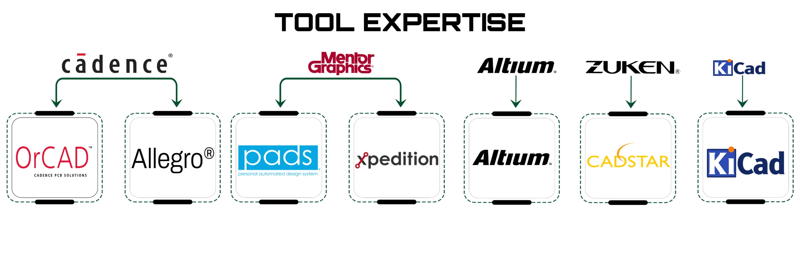
At TechiesDesigns, we specialize in PCB design to meet your project requirements. We are your end-to-end design-to-delivery partner. Our skilled PCB designers manage layouts efficiently while maintaining strict quality standards. We keep you informed throughout the design process, from schematic development to final delivery, using industry-leading tools such as Cadence, Altium, Mentor Graphics, and KiCad.
During layout development, our PCB design engineers work closely with circuit designers, mechanical engineers, and PCB manufacturers to ensure every board meets technical and manufacturing requirements.
Our clients trust us for handling complex designs with precision and reliability. Our experienced design team has successfully delivered projects across multiple industry sectors in India and beyond.
Why Choose TechiesDesigns for PCB Design?
Driven by Standards. Defined by Quality. Ready for Production.
-
Experienced PCB Design Experts
Skilled engineers with proven industry experience. Strong coordination with hardware, mechanical, and manufacturing teams. Deep knowledge of fabrication and assembly processes.
-
Advanced EDA Tools
Expert use of Altium, Cadence, and other leading platforms. Accurate schematic capture and PCB layout development. Robust ERC and DRC checks to prevent design errors.
-
Cost-Effective Engineering
Early DFM and DFA analysis to reduce redesign risk. Reuse of validated design blocks and libraries.
-
On-Time Delivery
Support for ECOs, revisions, and optimization requests. Design improvements for performance, cost, and manufacturability.
-
Clear Design Documentation
Complete and structured schematic and layout files. Well-organized design records for future maintenance.
-
Onsite and Offshore Design Support
Dedicated onsite engineers for close collaboration. Single point of contact for project management. Offshore teams for scalable and cost-effective execution.
-
Custom, Scalable, and Reliable Designs
Designs aligned with customer specifications and standards. Application-specific schematics and layouts. Solutions built for performance, manufacturability, and longevity.
-
Cost-Effective Engineering
Designs aligned with industry standards. Support for EMI, EMC, and safety requirements. Compliance with IPC design and manufacturing guidelines.
-
PCB Layout Updates and Modifications
Support for ECOs, revisions, and optimization requests. Design improvements for performance, cost, and manufacturability.
-
Production-Ready, Error-Free Designs
Strict adherence to DFM and DFA principles. Comprehensive design verification before fabrication.
Types Of PCBs We Design and Deliver
-
Single Layer PCBs
➥ Low manufacturing cost.
➥ Used in simple power supply circuits and low complexity devices. -
Double Layer PCBs
➥ Higher circuit density than a single layer.
➥ Used in industrial controls, amplifiers, automotive systems. -
Multilayer PCBs
➥ Reduced size and weight.
➥ High-density boards for complex routing and advanced electronic systems. -
Flexible PCBs
➥ Reduces connectors and wiring.
➥ Lightweight bendable circuits for compact and dynamic applications.
-
Rigid-Flex PCBs
➥ High reliability interconnections.
➥ Integrated rigid and flexible sections for space-saving and high-reliability designs. -
High-Frequency PCBs
➥ Minimal signal loss at high GHz ranges.
➥ Controlled impedance boards for RF, microwave, and high-speed signal transmission. -
HDI PCBs
➥ Reduces board size and weight.
➥ Fine-pitch, microvia-based boards for miniaturized high-performance electronic designs. -
Metal Core PCBs
➥ Used in LED lighting and power electronics.
➥ High thermal conductivity ensures efficient heat dissipation.
Our PCB Design Workflow
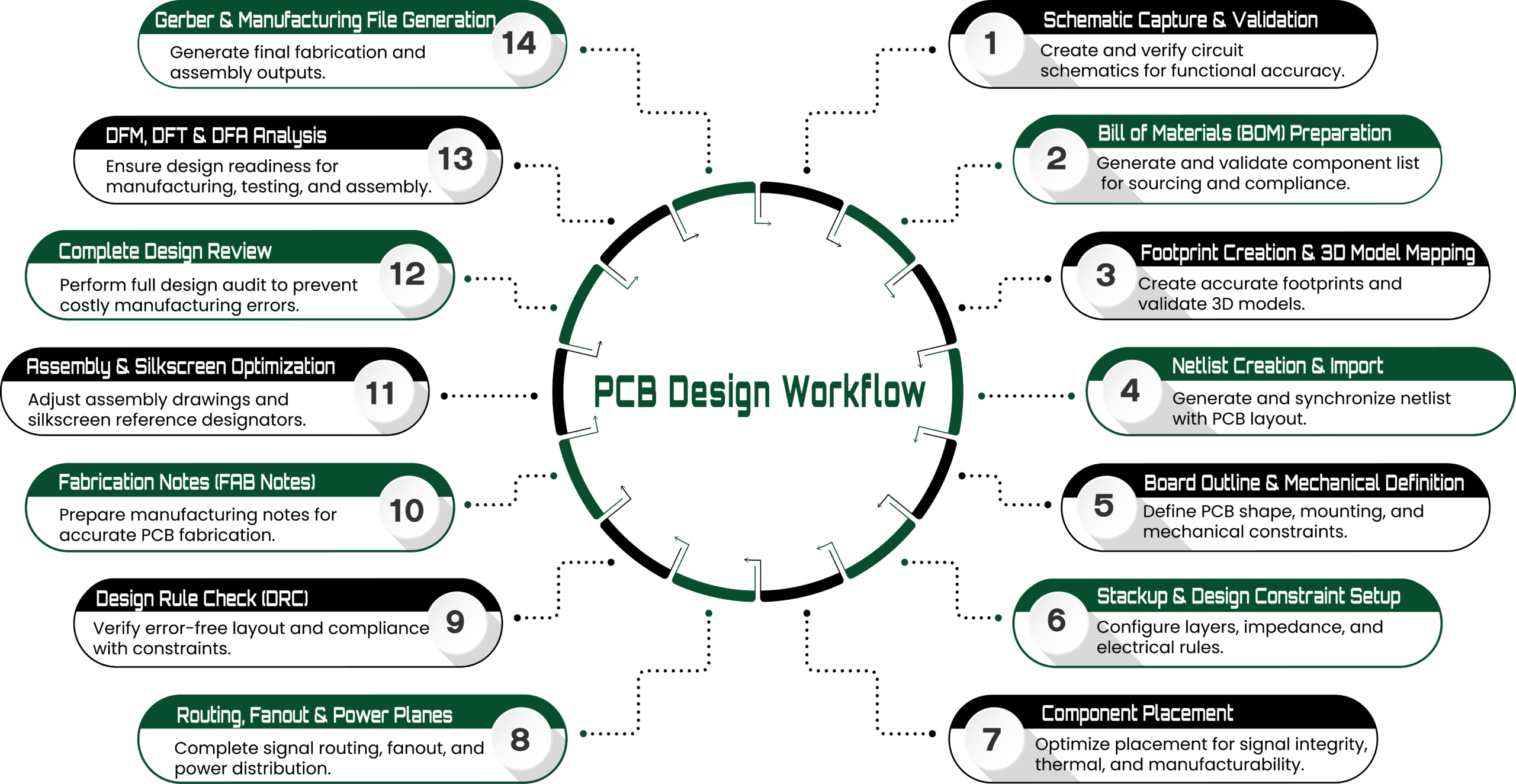
➥ Maintain a well-structured schematic symbol and PCB footprint library fully aligned with IPC standards, ensuring consistency, accuracy, traceability, and long-term reusability across projects.
➥ Design complex multi-layer PCBs for high-power motor controllers, DC-DC converters, inverters, battery management systems (BMS), RF modules, antenna layouts, and high-speed digital interfaces operating in the GHz range.
➥ Possess strong expertise in defining reliable, manufacturable PCB stack-ups, including rigid, flexible, and rigid-flex designs, ensuring optimal electrical performance, mechanical reliability, thermal stability, and cost efficiency.
➥ Optimize power planes, creepage and clearance distances, isolation barriers, and thermal dissipation paths for high-voltage and high-current designs, ensuring safety, performance, and compliance.
➥ Implement low-inductance routing, controlled impedance structures, and robust grounding schemes for high-power and high-speed circuits. Optimize layouts to minimize crosstalk, reflections, EMI, and insertion loss.
➥ Select appropriate PCB substrate materials such as FR4, Rogers, Polyimide, and high-Tg laminates based on performance, reliability, frequency, and environmental requirements. Implement microstrip, stripline, coplanar waveguide, and controlled impedance routing techniques.
➥ Apply EMI/EMC best practices, including shielding strategies, filtering networks, differential pair routing, star grounding, guard rings, Kelvin sensing, and noise isolation methods to achieve low-noise, high-integrity designs.
➥ Ensure compliance with IPC standards (IPC-2221, IPC-600, IPC-6012), EMI/EMC regulations, and applicable automotive, industrial, and safety certification requirements.
➥ Collaborate closely with RF engineers to optimize antenna layouts, RF routing, grounding strategies, and impedance matching, enhancing overall signal integrity and RF performance.
➥ Design low-noise precision analog layouts, including op-amp circuits, ADCs, DACs, sensor interfaces, and mixed-signal designs, ensuring minimized parasitic capacitance, inductance, and noise coupling.
➥ Work closely with mechanical engineers to optimize PCB form factor, enclosure integration, airflow, and cooling solutions, implementing thermal vias, heat sinks, copper pours, metal-core PCBs (MCPCB), and heat-spreading techniques for high-power designs.
➥ Demonstrate strong expertise in component footprint validation, 3D mechanical verification, and full PCB layout documentation prior to Gerber release.
➥ Generate manufacturing-ready Gerber RS-274X outputs, separate Excellon drill files for PTH and NPTH, detailed stack-up drawings, and complete fabrication notes covering materials, finishes, tolerances, impedance requirements, and special manufacturing instructions.
➥ Collaborate with PCB fabrication and assembly partners to ensure high-yield manufacturing, first-pass success, and production scalability.
PCB Design That Works – Case Studies & Proven Results
We provide complete manufacturing-ready design output files to ensure smooth and error-free production.
FABRICATION FILES
BOM
DESIGN FILES
ASSEMBLY FILES